Popular transistors.
MJE13003 and 13003 transistors.
Pinout.Datasheet.
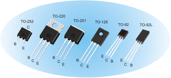
Marking: 13003,MJE13003. Attention! MJE13003 in packages TO-92 and TO-126 can have a different pin arrangement (not as in the first image)!
For example:
If the transistor is faulty in such a way that the location of its pins can't be specified by the multimeter
or tester, you need to pay attention to its connection to the electronic circuit of the device in which it is used.
Some 13003 contain built-in diodes connected between the emitter and the collector.
Their purpose is to protect the transistor from reverse voltage pulses that occur when
it operates with an inductive load-usually the transformer winding.
The main parameters of the 13003(MJE13003).
Material of transistor: Si
Power Dissipation (PD)at a collector temperature not exceeding 25° supported by a heat sink.(|Tc|=25° Collector-base breakdown voltage |VCBO|: 700 V. Collector-emitter breakdown voltage |VCEO|: 400 V. Emitter-base breakdown voltage |VEBO|: 7 V. Maximum Continuous collector current |Ic max|: 1,5 A . Maximum junction temperature |Tj|: +150 °C . Transition frequency (ft) : 10 MHz(min). Collector-emitter saturation voltage|VCE|:1 V(IC=1A,IB=0,25A),3 V(IC=1,5A,IB=0,5A). Base-emitter saturation voltage|VBE|:1 V(IC=0,5A,IB=0,1A),1,2 V(IC=1A,IB=0,25A). Forward current transfer ratio |hFE| : 14-57. Storage time|t s |:1 µs. Fall time |t F |:0,7 µs. |